- 您现在的位置:买卖IC网 > Sheet目录17350 > IRDC3841W (International Rectifier)BOARD EVAL FOR IR3841W 8A CONV
�� �
�
�IR3841MPbF�
�Layout� Considerations�
�Vin�
�PGnd�
�PGnd�
�capacitor� at� the� Sw� pin.�
�AGnd� Vout�
�The� layout� is� very� important� when� designing� high�
�frequency� switching� converters.� Layout� will� affect�
�noise� pickup� and� can� cause� a� good� design� to�
�perform� with� less� than� expected� results.�
�Make� all� the� connections� for� the� power�
�components� in� the� top� layer� with� wide,� copper�
�filled� areas� or� polygons.� In� general,� it� is� desirable�
�to� make� proper� use� of� power� planes� and�
�polygons� for� power� distribution� and� heat�
�dissipation.�
�The� inductor,� output� capacitors� and� the� IR3841�
�should� be� as� close� to� each� other� as� possible.�
�This� helps� to� reduce� the� EMI� radiated� by� the�
�power� traces� due� to� the� high� switching� currents�
�through� them.� Place� the� input� capacitor� directly� at�
�the� Vin� pin� of� IR3841.�
�The� feedback� part� of� the� system� should� be� kept�
�away� from� the� inductor� and� other� noise� sources.�
�The� critical� bypass� components� such� as�
�capacitors� for� Vcc� should� be� close� to� their�
�respective� pins.� It� is� important� to� place� the�
�feedback� components� including� feedback�
�resistors� and� compensation� components� close� to�
�The� connection� between� the� OCSet� resistor� and�
�the� Sw� pin� should� not� share� any� trace� with� the�
�connection� between� the� bootstrap� capacitor� and�
�the� Sw� pin.� Instead,� it� is� recommended� to� use� a�
�Kelvin� connection� of� the� trace� from� the� OCSet�
�resistor� and� the� trace� from� the� bootstrap�
�Vin�
�VoutAGnd�
�In� a� multilayer� PCB� use� one� layer� as� a� power�
�ground� plane� and� have� a� control� circuit� ground�
�(analog� ground),� to� which� all� signals� are�
�referenced.� The� goal� is� to� localize� the� high�
�current� path� to� a� separate� loop� that� does� not�
�interfere� with� the� more� sensitive� analog� control�
�function.� These� two� grounds� must� be� connected�
�together� on� the� PC� board� layout� at� a� single� point.�
�The� Power� QFN� is� a� thermally� enhanced�
�package.� Based� on� thermal� performance� it� is�
�recommended� to� use� at� least� a� 4-layers� PCB.� To�
�effectively� remove� heat� from� the� device� the�
�exposed� pad� should� be� connected� to� the� ground�
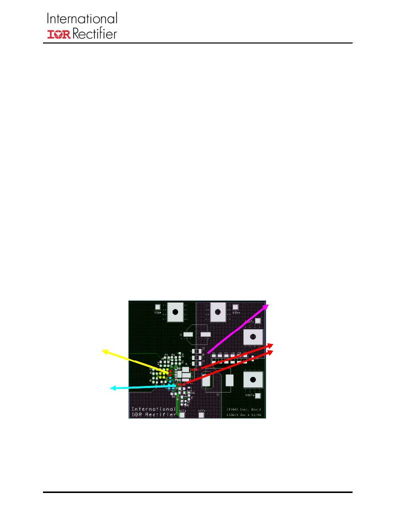
�plane� using� vias.� Figure� 25� illustrates� the�
�implementation� of� the� layout� guidelines� outlined�
�above,� on� the� IRDC3841� 4� layer� demoboard.�
�Fb� and� Comp� pins.�
�Enough� copper� &�
�minimum� length�
�ground� path� between�
�Input� and� Output�
�PGnd�
�Compensation� parts�
�should� be� placed� as� close�
�as� possible� to�
�the� Comp� pin� .�
�Vin�
�Vin�
�PGnd�
�All� bypass� caps�
�should� be� placed� as�
�close� as� possible� to�
�their� connecting�
�pins.�
�AGnd�
�Resistors� Rt� and�
�Rocset� should� be�
�placed� as� close� as�
�possible� to� their� pins.�
�AGnd�
�Vout� Vout�
�Fig.25a.� IRDC3841� demoboard� layout�
�considerations� –� Top� Layer�
�06/18/09�
�27�
�发布紧急采购,3分钟左右您将得到回复。
相关PDF资料
TARQ474M035
CAP TANT 0.47UF 35V 20% AXIAL
GCM06DCCN-S189
CONN EDGECARD 12POS R/A .156 SLD
A9CAA-0803E
FLEX CABLE - AFK08A/AE08/AFH08T
A9BBA-1002E
FLEX CABLE - AFJ10A/AE10/AFJ10A
GCM06DCCH-S189
CONN EDGECARD 12POS R/A .156 SLD
EEM15DSXI
CONN EDGECARD 30POS DIP .156 SLD
GCM06DCCD-S189
CONN EDGECARD 12POS R/A .156 SLD
SJP7401-4-50-BLACK
LOOP BLACK 4" X 50YD X 0.11"
相关代理商/技术参数
IRDC3842
功能描述:电源管理IC开发工具 IR3842 SYNC CONV 600kHz EVAL BRD RoHS:否 制造商:Maxim Integrated 产品:Evaluation Kits 类型:Battery Management 工具用于评估:MAX17710GB 输入电压: 输出电压:1.8 V
IRDC3842A
功能描述:电源管理IC开发工具 IR3842A SYNC CONV 300kHz EVAL BRD RoHS:否 制造商:Maxim Integrated 产品:Evaluation Kits 类型:Battery Management 工具用于评估:MAX17710GB 输入电压: 输出电压:1.8 V
IRDC3842W
功能描述:电源管理IC开发工具 User Guide IR3842W Eval Brd RoHS:否 制造商:Maxim Integrated 产品:Evaluation Kits 类型:Battery Management 工具用于评估:MAX17710GB 输入电压: 输出电压:1.8 V
IRDC3843
制造商:International Rectifier 功能描述:BOARD EVALUATION IR3843
IRDC3843A
功能描述:电源管理IC开发工具 IR3843 SYNC CONV 600kHz EVAL BRD RoHS:否 制造商:Maxim Integrated 产品:Evaluation Kits 类型:Battery Management 工具用于评估:MAX17710GB 输入电压: 输出电压:1.8 V
IRDC3843W
功能描述:电源管理IC开发工具 User Guide IR3843W Eval Brd RoHS:否 制造商:Maxim Integrated 产品:Evaluation Kits 类型:Battery Management 工具用于评估:MAX17710GB 输入电压: 输出电压:1.8 V
IRDC3853
功能描述:电源管理IC开发工具 User Guide IR3853 Eval Brd RoHS:否 制造商:Maxim Integrated 产品:Evaluation Kits 类型:Battery Management 工具用于评估:MAX17710GB 输入电压: 输出电压:1.8 V
IRDC3853 - SUPIRBUCK
制造商:International Rectifier 功能描述:INTERNATIONAL RECIFIER - GEN 2.1 SUPIRBUCK FAMILY - Bulk